We have expertise in Nanoscale Electronic and Optoelectronic Device Fabrication in a cleanroom environment utilizing E-Beam Lithography, Nanoimprint Lithography and Photo Lithography.
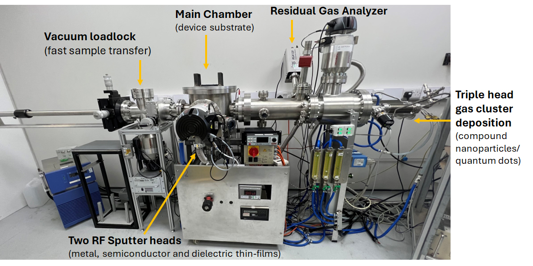
Unique Multilayer Memristor Deposition System
We have designed and developed a unique Multilayer Memristor Deposition System that allows the deposition of multilayer thin-film stacks (metals/semiconductors/insulators) with embedded nanoparticle/quantum dots under high vacuum conditions. The system is equipped with a heated stage, a residual gas analyzer and a vacuum loadlock for fast sample transfer.
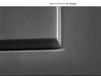
Some examples of our fabricated devices are shown below:
Combined Nanoimprint Lithography + Photolithography


Bi-Layer Nanoimprint Lithography

(note: a specific advantage of using the bi-layer approach is the ability to undercut the edge of the PMMA layer to improve lift-off )
Single Layer Nanoimprint Lithography

Si Wafer Diced Devices

